
I've been mulling over the F35 inside when I have it apart, just wondering how it all works. On the side of the inside of the CCD block is a set of 2 potentiometers. I don't think it would be a good idea to play with these but what if it's a magical turn down the noise switch. Haha, probably not but they are there to fine tune a voltage which I find interesting.
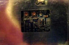
Also another interesting thing on the CCD block is the two circles cut around these two components specifically, for heat? Or they fail earliest on the F35's so they left the hole for easy access.
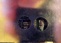
I think JM said in another thread that the dip switch on the CCD block is for the powered lens upgrade. Which the Pots could be related to that also.
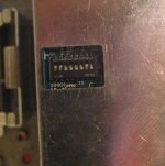
I believe the "motherboard" of the F35 is referred to as the CHU according to labels on the boards. The motherboard or CHU connects to all the boards and the CCD and on the other side connects to the SDI output board.
What do the 4 main boards do? The furthest back board is connected to the power supply and distributes power throughout the camera. The next card AT has two wires that only run to the ethernet, I'm tempted to see if the camera will run without this board if it is only the "ethernet card" component of the F35 computer. VDA who knows? AD is a connection to the CCD and motherboard. The ccd connects to the motherboard directly, the AD card, and the power supply card.
I know this isn't very helpful to anyone, I wish I was a much smarter engineer to reverse engineer this camera and find the 6k raw file. I don't think the image from the F35 is lacking, but I wonder if there is a little more to be squeezed out if the HD file size is a bottleneck.
The space dedicated to the memory stick reader and empty space behind it is massive. Makes me wonder if something like the new ninja star without the case would fit in there, modify the memory stick hole to fit a CF card.
Also another interesting thing on the CCD block is the two circles cut around these two components specifically, for heat? Or they fail earliest on the F35's so they left the hole for easy access.
I think JM said in another thread that the dip switch on the CCD block is for the powered lens upgrade. Which the Pots could be related to that also.
I believe the "motherboard" of the F35 is referred to as the CHU according to labels on the boards. The motherboard or CHU connects to all the boards and the CCD and on the other side connects to the SDI output board.
What do the 4 main boards do? The furthest back board is connected to the power supply and distributes power throughout the camera. The next card AT has two wires that only run to the ethernet, I'm tempted to see if the camera will run without this board if it is only the "ethernet card" component of the F35 computer. VDA who knows? AD is a connection to the CCD and motherboard. The ccd connects to the motherboard directly, the AD card, and the power supply card.
I know this isn't very helpful to anyone, I wish I was a much smarter engineer to reverse engineer this camera and find the 6k raw file. I don't think the image from the F35 is lacking, but I wonder if there is a little more to be squeezed out if the HD file size is a bottleneck.
The space dedicated to the memory stick reader and empty space behind it is massive. Makes me wonder if something like the new ninja star without the case would fit in there, modify the memory stick hole to fit a CF card.
