F5: F5/F55/FS7 Sensors...

JMtheDP

Veteran
Does anyone know why there is a large difference between the actual pixel count on these cameras (11.9MP) and the used pixel count (8.9MP)?

I wonder if they are natively 4:3 sensors, perhaps pinched from something else? That would explain the difference.... also does anyone know how closely related they really are? I appreciate there are differences, even between the F5 and 55 but how much of it is "tacked on" stuff, and how much of it is fundamentally different engineering?
 
Given the identical photosite count between them, I get the impression it's the exact same sensor, only the F55 has the CFA from the F65 added in front of it (where the F5/FS7 have a less advanced CFA in front of theirs). And the F55 has the global shutter architecture behing it.
 
See Sony had led me to believe that the F5 and F55 were a fundamentally different sensor, due to the global shutter thing... but I'm wondering how much that is the case? Or perhaps they just share a common design?
 
The pixels counts are the same yes, but if I remember correctly the F55 has smaller pixels than the F5/FS7 across the same surface area. The reason they are smaller is because additional space is used to accommodate small electronic "swiches" or "gates" which is how the F55 accomplishes "global shutter". Hence also why the native ISO of the F55 is 1250, ie. it is less light sensitive because of smaller pixels.

So the F55 is really a different sensor the way I look at it.

Was it ever confirmed it the FS700 sensor same as F5/FS7?
 
Very interesting that the Sony F35 has 12.44MP effective, and the current gen FS7, F5, and F55 all only have 8.9MP effective. Might be interesting to compare max outputs for each camera for green screen compositing. I would think that the F35 would remain competitive, despite only outputting 12bit RGB 444 1080p.
 
I think Viddo the F35 would reign supreme against nearly anything for 1080P pictures - especially green screen work.

The F5 and F55 would probably be at their best shooting raw or XAVC, then doing the work, then downconverting - but you'll always have a slight softness to the picture.
 
Interesting that Sony eventually published the actual sensor res of the F3 - that was a big secret for a long time.

I imagine the F5/F55/FS7 sensor must have begun life as a stills camera chip, but presumably with radically different electronics.

I wonder how much of the sensitivity loss of the 55 is due to the global shutter and how much is the CFA?
 
Does it have to do with the De-bayer? The actual pixels for the sensor are 25% to 33% greater than the recorded pixels due to the de-bayer process or downsampling. That would be my guess.
 
Does it have to do with the De-bayer? The actual pixels for the sensor are 25% to 33% greater than the recorded pixels due to the de-bayer process or downsampling. That would be my guess.

As JMtheDP says, this isn't the case, not really. Effective photosites means all used photosites, without regard to color filtering. We say effective, because virtually always image sensors have additional photosites on the edges that are not actively used. This is for a variety of reasons, including production cost issues as well as internal camera utility functions.

However, you do *almost* get at something. If we take 4096 and multiply it by 2160 (4096x2160 being the largest available output resolution of the FS7/F5/F55) you get 8,847360. You round that and you have 8.8MP. If you increase the dimensions to 4098 by 2162, you get 8,859,876 - which would round up to 8.9MP. So, presumably, Sony is 1 to 1 mapping color filtered photosites to entire output pixel locations in 422 color space. There are many ways to choose to interpret a Bayer sensor grid, but this is one of them - you essentially take the known color value for each photosite (whichever color was collected), and then add values for the other two colors from the adjacent surrounding pixels. Since using only 4096x2160 would mean the edge pixels don't have references on all sides, you add an extra row or column on the left, right, top, and bottom of the sensor. These new edges - 4098x2162 - aren't given full mapped values, but used to help generate the 4096x2160 output edge values.

Mind you, I'm sure the actual process has some secret sauce I'm not covering here, but this would be the most sensible explanation I can think of for why it's an 8.9MP effective sensor. The math works.

The sensor is delivering 422 at the very best, and even that is pushed, I would think. Even at 1080p it's only got 4 photosites to use before interpolation, meaning 2 green, 1 red, and 1 blue. That's enough to make 4:4:4, but not any better than that 444 from the F35 (and quite possibly worse), which uses 6 photosite (2red, 2green, 2blue) to derive it's 444 values.
 
... I imagine the F5/F55/FS7 sensor must have begun life as a stills camera chip, but presumably with radically different electronics. ...
IMO, all the niche products are basically heavily modded mass production models. Hypothetically, one could take any FF sensor - even from something like RX1 - and add a bunch of processing power with an improved signal path and get a terrific high end/pro product.

PS. Many years ago, when I was selling audio, I recall someone taking a screwdriver and adjusting the playback head alignment on a middle of the road Technics tape deck, instantly turning it into a high end performer. Even today, folks mod everything from amps to CD players by changing the caps, the resistors, the rectifiers, the tubes, the clocks and so on. This is obviously a gross oversimplification as the sensor mods have to be quite extensive but the general idea is the same.

There are limiting factors, but there's a lot of truth here.

Not all sensors have the same room for output improvement though. Different image sensors have different hard limits on a variety of factors, but one of the most important is how fast they can output data. In a stills world this is less of a factor (although many stills photographers appreciate fast burst modes), but for video, your might as well consider the best quality of the image sensor to be what it can put out in less than 1/30th of a second (or perhaps, 1/24th).

In essence, an image sensor is an integrated circuit, with inputs and outputs, and permissible clock speeds. The max clockspeed and the nature of the data output (serial, parellel, etc) puts a hard cap on allowable speeds. In practice, one also ends up dealing with the caps on other components in the path. But these data transfer caps are one of the reasons why high speed readouts of the sensors frequently take crops of the sensor, or bin the sensor in half. By instructing the sensor to only output a fraction of what it sees, more frames of data can be sent per second.


As for the fact that cheaper consumer goods frequently use some of the same parts as high end goods - absolutely. But even if they use the same parts, there often isn't the same degree of quality control applied - hence why one might drastically improve performance by merely twisting a pot or adjusting a playback head alignment.

For image sensors, not every unit manufactured performs equally. In the quality control process they will frequently divide the chips into performance grades. Some will be outright rejects, while others will be good enough for the consumer goods, with the ones getting the best QC grades being reserved for the highest end products. So just because the FS7 and FS700 share the same chip as the F5 doesn't mean that all three cameras receive chips that performed to the same QC grade. RED absolutely did/does this with Scarlet and EPIC MX.
 
Does anyone know why there is a large difference between the actual pixel count on these cameras (11.9MP) and the used pixel count (8.9MP)?

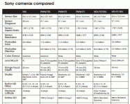
It's actually 11.6, not 11.9. Furthermore if you sift through lots of brochures and technical specs you'll find some mention 4352 x 2662 (11.6 MP).

I wonder if they are natively 4:3 sensors

4352 x 2662 is a ratio of 16:10, so I guess not.

also does anyone know how closely related they really are?

sony_cameras_compared.gif

(from F5 brochure, p. 11)

The F65 is the odd duck, with a Q67 bayer pattern. You can't just put that pattern on anything. The chip must be made for it, literally rotated 45 degrees. Therefore it ends up being useless as RAW. The advantage, however, is that you can get 4:4:4 RGB from just twice as many photosites as your output resolution. It gets 4:4:4 4K from just 16 megapixels. Before the best you could do if you wanted true 4:4:4 RGB was three times as many photosites, as with the rare RGB-striped CCD like in Sony's F35. Or you could always get 4:4:4 from a normal Bayer pattern, with quadruple the pixel count (a 4K-by-2K Bayer sensor could give true 2K-by-1K 4:4:4 RGB). So, Q67 is the most efficient if you care about 4:4:4 RGB output.
 
Last edited:
I can't recall reading exact specs for the total sensor resolution on the F5/55. That would be interesting if those were the numbers - 16:10 is a very odd aspect ratio for a sensor, although it is not far off 3:2 so perhaps not so surprising. I've had S35 on the brain and been confusing that ratio with the FF / Leica frame.

The F65 I believe loses about 800,000 pixels from the total sensor if the 20MP figure is accurate. 8192 x 2160 is about 19.2MP. I imagine this is partly due to the Q67 being difficult around the edges and partly Sony blanking off those pixels for calibration reasons.

I've seen that brochure before and that was the reason for my question - Sony would have us believe (or have told me to my face) that the F5 and F55 are very different things - but looking at the basic specs of sensor size, res and photosites they seem eerily similar - and that extra wasted 3MP still bugs me. That's way more than normal. If they were using them for a better 4K picture, they would definitely shout about them.

EDIT: I found that resolution mentioned in the brochure for the FS700. They mention several times there it being an "11.6MP" sensor. I wonder if that is a marketing thing because they're going for this DSLR-type audience who would most likely look down on something with a single digit MP count. Still very cheeky on Sony's part, as the FS700 clearly isn't using the whole sensor either.
 
Last edited:
You're right, three million pixels is a lot to lose. I don't know why those sensors have so many extra.

On a related note, I am tempted to look for matches among cameras: if the chips in two cameras have the same size and pixel count, I'm tempted to think they are the same sensor. But I have to remember that Sony makes its own sensors, and they can repeat certain specs over and over. For whatever reason they may decide to make two or three sensors with the same size and pixel count, but which differ in dynamic range, global shutter, etc.
 
There are limiting factors, but there's a lot of truth here.

Not all sensors have the same room for output improvement though. Different image sensors have different hard limits on a variety of factors, but one of the most important is how fast they can output data. In a stills world this is less of a factor (although many stills photographers appreciate fast burst modes), but for video, your might as well consider the best quality of the image sensor to be what it can put out in less than 1/30th of a second (or perhaps, 1/24th)...

You're right, three million pixels is a lot to lose. I don't know why those sensors have so many extra.

On a related note, I am tempted to look for matches among cameras: if the chips in two cameras have the same size and pixel count, I'm tempted to think they are the same sensor. But I have to remember that Sony makes its own sensors, and they can repeat certain specs over and over. For whatever reason they may decide to make two or three sensors with the same size and pixel count, but which differ in dynamic range, global shutter, etc.

Let me bridge the difference - if any exist to begin with - between us. There has to be some sort of a modular manufacturing process where an X-sensor of a certain size is made with so many pixels and to a certain mathematical requirement but then there's enough room, left there by intent, to offer the various performance upgrades in terms of clock speed, buffer, signal paths, etc. In some cases, this may not be possible - as James says, there are limits - but, even with Canon C 100/300 line, a seeming impossible upgrade to DPAF was.

To me, this does smack of an automotive industry where one can get a 305 HP 4-cylinder Ecoboost Mustang for ~ $27,000 and a 525 HP Shelby version for twice the price. It's essentially the same model but with a very wide range of performance. On the high end, it won't turn into a 911 but obviously the gap between the bottom and the top of the line is pretty huge. Cars may be far more modular in that regard than cameras and their sensor components but we see how much improvement an external recorder - i.e,., the recording bit rate and the codec - can make to an image quality. That makes me think that the innate sensor variances within a given line from a particular manufacturer may not be as large as once thought.
 
To me it seems pretty obvious that Sony's marketing people use the 11.6 number simply because it sounds good - most people don't understand how image sensors actually work, but the idea of more sounds better. From the engineering side though, I don't think there's any conspiracy. Firstly, the photosites that are not part of the effective image path are used for a variety of automated calibrations. Secondly, as we've seen, image sensors are recycled and reused in multiple camera models. In many cases, the image sensor is (despite my prior post) capable of higher output than the circuitry behind it is capable of handling. Thus, as it becomes practical in cost, size, heat, and performance to handle more of the chip's output capacity newer camera models are released with the upgraded processing for the same old imager chip. The RED ONE MX and RED EPIC share the same chip that has a 5120x2700 pixel array... The Red One MX max active area of that chip was 4480x2304 (or 10.3MP), while the newer, more compact and more advanced EPIC was able to use the entire array. RED considers the 4480x2304 of the Red One MX to be "4.5k", which, counting across, it essentially is. But that means RED is also considering 8.9MP of photosites to be 4k. So if anything, Sony developed a sensor that just like the RED MX sensor, can be made to support 5k in future releases. They thought ahead.

It's also possible the Sony will use those photosites for features like digital stabilization or viewfinder "look-around" (non recordable, but viewable for framing - like an optical viewfinder) on future cameras.

The Sony F55 has been shown to output 360fps via special hardware - the chips are clearly capable of far more than the current internal circuitry supports. Sony will likely use and reuse these sensors designs for a number of camera iterations, focusing on improvements in processing, size, and heat. It's a smarter practice than making a new chip each time.
 
Last edited:
Back
Top